Electronic skin
Research thrust overview
Electronic skin exhibits seamless integration of perception, control, communications, and energy at multiple scales in soft robotic systems and interaction with the human body. Distributed functions in application-driven systems stretch and flex with user (or robot, or object) movement while maintaining robust end-use function and performance. Applications include health and vital sign monitoring, and high-fidelity tactile sensing and haptic actuators for closed-loop human-machine interfaces.
Thrust projects described below include:
- GelSight tactile sensing
- Photonic tactile sensors
- Stretchable 3D-printed circuit board process
- Aerosol-jet printed sensors
- ElectroDermis
GelSight tactile sensing
We have been working on developing and applying a vision-based high-resolution tactile sensor called GelSight. A GelSight sensor measures the detailed geometry of objects being touched, including surface textures. It also measures the shear forces and torques at the contact surface. Therefore, a robot could use GelSight sensors to precisely detect touch and relevant contact information. It can use the information to have a good understanding of the physical environment and guide better manipulation. In the future, we expect the high-resolution tactile sensing provided by GelSight can help robots to perform more intelligently and work with humans. Particularly, the core sensing part of the GelSight sensor is a soft elastomer so that the sensor design could be adapted to soft robots. Our current work focuses are exploring new design, materials, and fabrication of the GelSight sensors, improving the modeling of the sensor, and applying the sensors on robots for perception and manipulation tasks. The following video shows a robot using tactile feedback from GelSight to detect large torque when grasping long objects. The robot could use the feedback to update grasp strategy and enable stable grasps.
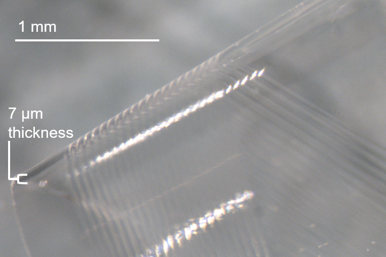
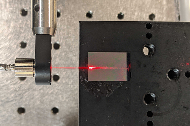
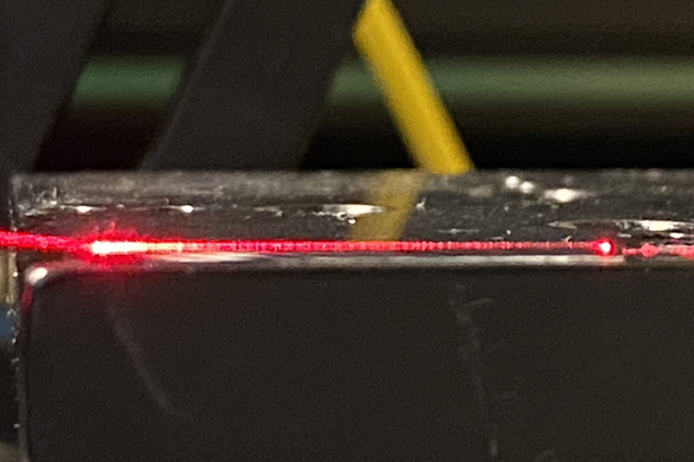
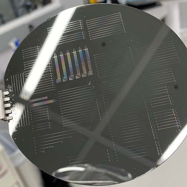
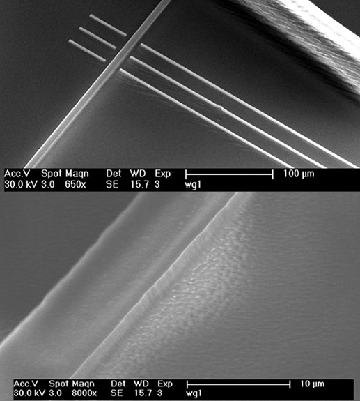
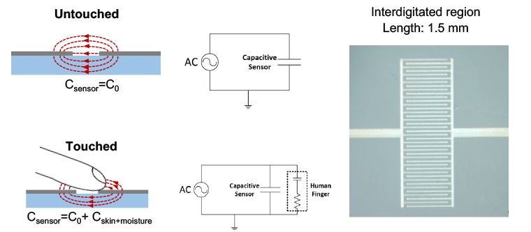
Photonic tactile sensors
The project aims to develop a large-scale flexible tactile skin, which can measure contact with a high spatial resolution of 100um. The tactile skin could be used on traditional and soft robots for dexterous manipulation tasks and wearable sensors to monitor human health conditions. We will build the sensor using optical methods by designing an array of optical interferometers made of novel Parylene C photonic waveguides embedded in a PDMS cladding. The tactile input, which usually poses a distribution of normal force and normal displacement on the surface, can be accurately measured through the interference readouts of the waveguides. Our project will focus on designing, modeling, and manufacturing the densely packed microscale sensing units in large arrays. Compared to existing tactile sensors, the new sensor has the advantages of structural flexibility, high resolution, biocompatibility, and covering large areas. Those will make the sensor suitable for the large and curved surfaces of robots and human bodies, especially for soft robots where traditional sensors can hardly be applied. The pictures show examples of our fabrication process and the testbed of the micro waveguides.
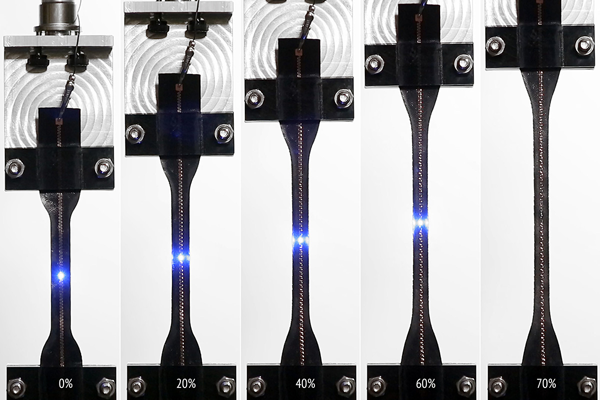
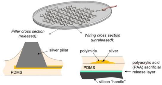
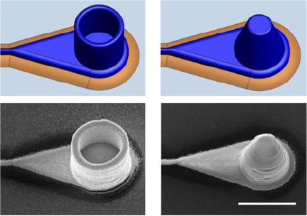
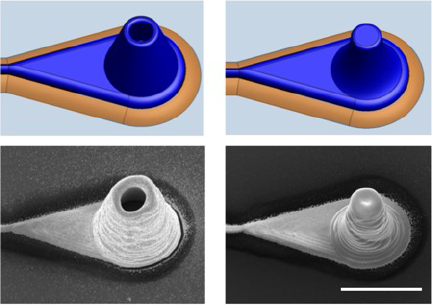
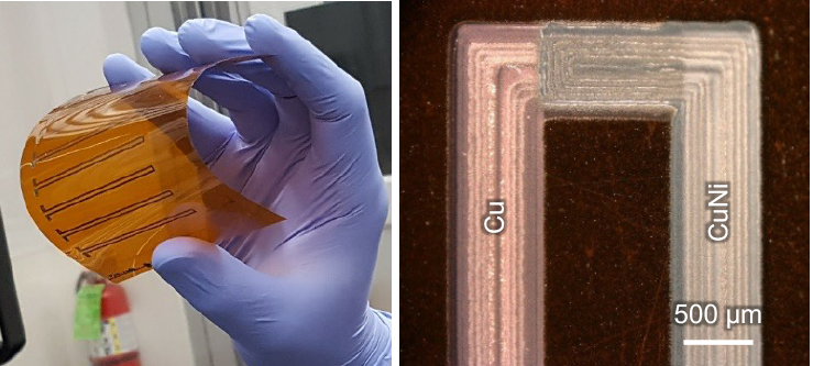
Stretchable 3D-printed circuit board process
We are developing an end-to-end process flow to make stretchable interconnect in elastomeric substrates like polydimethylsiloxane (PDMS) that extends to multiple interconnect layers and can connect to sub-mm-sized electronic and sensor chips. The end result are direct 3D-printed stretchable multi-layer printed circuit boards that become a foundational process for electronic skin applications. Interconnect is made through aerosol-jet printing steps forming polyimide-silver-polyimide layers. 3D pillars enable external electrical connection to the surfaces of the PDMS substrate. Aerosol jetting the metal nanoparticles can form a myriad of 3D conductive shapes, such as vertical hollow cylinders and solid tapered pillars. Stiffness gradients can be designed in the substrate to assist with inhibition of delamination of interconnected components embedded in the PDMS.
Video of 3D-printed circuit board interconnect, stretched in an Instron machine until failure. Left: 135° meander wiring. Center: 180°meander wiring. Right: 270° meander wiring.
Aerosol-jet printed sensors
Multi-material 3D printing of metals, ceramics, and polymers at micron scale enables sensors to be fabricated directly on complex surface substrates and integrated with the stretchable circuit printed with the same aerosol jet process. Utilizing the aerosol jet process for both electrical interconnection and sensor fabrication can simplify device fabrication to utilize a single process. Temperature sensors, touch sensors, and 3D microstructures are example sensor applications fabricated via aerosol jet printing.
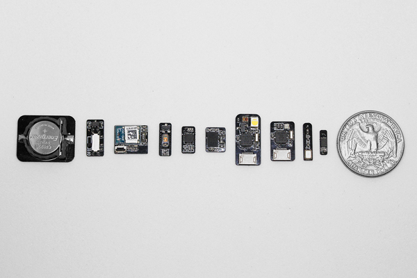
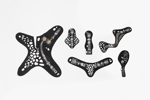
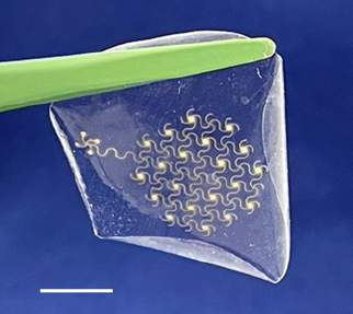
ElectroDermis
In addition to aerosol-based additive manufacturing, we are also developing methods to produce sticker-like wearable electronics using laser-based rapid prototyping. These stretchable circuits are composed of digital electronics that are wired together with serpentine interconnects and mounted on a soft elastic fabric that adheres to the skin. The electronic components are used for sensing, signal processing, wireless communication, and power and the interconnects are patterned using UV laser micromachining. This manufacturing method is compatible with a wide range of microelectronic architectures and can be used to create wireless sensing stickers that track body motion, physiological state, and health vitals. In addition to advancing novel prototyping methods, we are also developing computer-aided design tools that allow non-experts to produce sensing stickers that are customized to their needs. Together, these tools allow for rapid design, fabrication, and deployment of body-mounted wireless electronics in under an hour.