
Beyond silicon: Atomically thin transistors could transform computing
Carnegie Mellon researchers have demonstrated that wafer-scale transistors, less than 5nm long, surpass silicon’s switching limit. This finding showcases the potential for more energy-efficient computing beyond silicon.
For decades, silicon transistors have driven computational power, and scientists have devoted much of their time to making them smaller. That is because shrinking these tiny electronic switches that make up computer chips allows manufacturers to pack more of them into the same space, increasing computing power.
But as silicon transistors approach just a few nanometers in size, the material that has enabled decades of technological progress is threatened by fundamental physical limits.
Researchers at Carnegie Mellon University have now demonstrated that another class of semiconductors could shrink transistors beyond those limits.
In a study published in Nature Communications, the team built transistors from molybdenum disulfide, MoS₂, an atomically thin, two-dimensional semiconductor. The transistors had physical channel lengths below five nanometers and demonstrated switching performance beyond the theoretical limit of silicon at a comparable size.
A transistor works by controlling the flow of electrical current between an “on” and “off” state. As silicon transistors become extremely small, the gate that controls the current begins to lose its ability to completely shut the device off. Electrons can therefore leak through the transistor, even when it’s supposed to be off. This causes energy waste.
“We need to rethink semiconductor materials, especially in the era of AI computing,” said Xu Zhang, associate professor of electrical and computer engineering and corresponding author of the study. “What this work shows is that the limits of silicon do not necessarily have to be the limits of transistor technology.”
For that reason, the team turned to MoS₂.
This new material can experimentally break silicon’s limit.
Xu Zhang, Associate Professor, Electrical and Computer Engineering
“This new material can experimentally break silicon’s limit,” said Zhang. “This is the first time that’s ever been done.”
At nano-size dimensions, every piece of the transistor affects performance. Therefore, the researchers used a co-design technology to develop and co-optimize the material, device architecture, and fabrication process together.
“A material can’t automatically translate its properties into performance,” said Sheng Shen, professor of mechanical engineering and corresponding author of the study. “It needs innovative ideas on how to design the right device structure so that the benefits can be realized.”
The team’s breakthrough innovation was an air gap below the transistor channel. The air gap helps the transistor’s gate to maintain greater control over the current to reduce leakage.
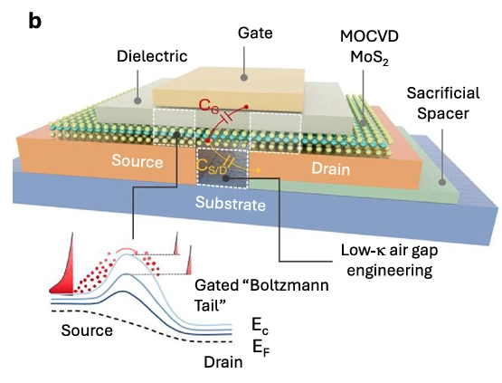
Schematic illustration of the device’s architecture
Additionally, the researchers fabricated the transistors across a four-inch wafer. This proves that the technology can eventually be produced at scale for manufacturing, rather than just on a single nanoscale device in a lab.
“Today, a majority of electronics for computation are based on silicon,” said Shen. “In the future, it’s going to be very different.”
While the device isn’t ready for commercialization yet, this research indicates that reaching silicon’s physical limits doesn’t necessarily mean the end of smaller, more efficient transistors. Instead, the future of computing may rely on new materials, designs, and more creative assembly.
This research was conducted in collaboration with The Massachusetts Institute of Technology, The University of Florida, Texas A&M, The University of Southern California, and Universidad Politecnica de Madrid.