
Scalable manufacturing unlocks potential of soft electronics
New research from Burak Ozdoganlar, Carmel Majidi, and Kadri Burga Ozutemiz seeks to develop a scalable manufacturing method that combines the best of quality and quantity on a miniature scale, with the potential to reimagine how wearable medical devices are made.
The classic conundrum of quality or quantity is perhaps never more important than in manufacturing, particularly when seeking to produce millions of units on a miniature scale. Burak Ozdoganlar and Carmel Majidi, both professors of mechanical engineering, have worked to create a reproducible and scalable manufacturing method for liquid metal circuits. Their approach could pave the way for the streamlined commercialization of soft and stretchable electronics (SSEs). Such soft and stretchable circuits find applications in a range of wearable electronics, non-invasive medical devices, and other applications that require circuits to conform surfaces and function under significant deformation.
Ozdoganlar explained why reproducibility in manufacturing is crucial. “To be able to make a marketable product, we must be able to make each one of these circuits with precision and consistency. Otherwise, one device is going to behave very differently from another device, and that’s not a product,” he said.
To be able to make a marketable product, we must be able to make each one of these circuits with precision and consistency. Otherwise, one device is going to behave very differently from another.
Burak Ozdoganlar, Professor, Mechanical Engineering
Liquid metal-based soft and stretchable circuits hold much potential for various applications because of their ideal physical and chemical properties. These liquid metals are gallium alloys, which are liquid at room temperature, have high electrical conductivity, and are non-toxic. In these circuits, the liquid metal is encapsulated in carefully designed micro-scale channels inside soft, rubber-like materials. This soft packaging can be tuned to possess mechanical properties similar to those of human skin, for example. When the circuits are stretched and deformed, the liquid metal retains the electrical connections by flowing inside the channels. These circuits could be made solely of liquid metals, including strain sensors, inductor elements, or antennas. Alternatively, liquid metal traces can be used as flexible interconnects, and traditional IC chips can be incorporated into the circuits. Notably, these circuits are incredibly durable: Part of the research experimentation involved stretching the circuits thousands of times, and they were found to maintain their full functionality even when deformed significantly.
The team, which included Kadri Burga Ozutemiz, who was then a Ph.D. candidate working on this project, had its findings published in Advanced Materials Technologies. While decades of research on liquid metal circuits have demonstrated the tremendous potential of liquid metal circuits and their various applications, a manufacturing technology that can produce millions of such circuits reproducibly and at a low cost has been lacking. To address this need, the research team has combined the effects of dip coating and surface alloying in a new method called SMAW-DC.
SMAW-DC uses lithography alongside the combined effects of selective metal-alloy wetting (SMAW) and wafer-level dip coating (DC). According to their paper, such a breakthrough in scalable manufacturing would be a long time coming because “despite significant progress over the past two decades, scalable, industrially-applicable manufacturing of SSEs remains a critical research challenge,” which prompted the team to develop the new process.
To begin, a silicon wafer is coated with an elastomer, a polymer that provides both softness and flexibility. Next, using photolithography, very thin traces of copper or gold are deposited onto the desired locations of the elastomer, serving as the template for the geometry of the electronic circuit. Then the circuit is dipped into a liquid metal bath to selectively deposit the liquid metal on the wafer in a specific pattern with a thin copper film. The team chose gallium-based liquid metals for their research because they are stable and conducive for application in microelectronics. This selective liquid-metal deposition happens through alloying between the thin copper traces and the gallium-based liquid metal. The IC chips, if desired, are added to the circuit. A final layer of elastomer is then used to seal the circuit.
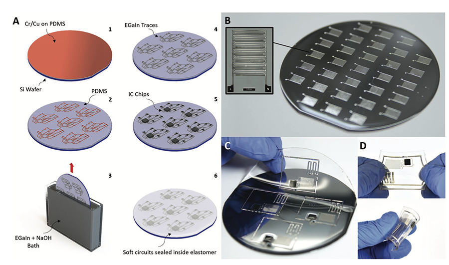
A closer look at the dip-coating process.
“One of the most important things is that these process steps can be integrated into the existing lithographic processes,” Ozdoganlar says, emphasizing the system’s potential for scalability and commercial appeal. These lithographic processes are used to make billions of computer chips: Integrating the SMAW-DC into the existing lithographic processes will ensure high-volume manufacturability of SSEs.
Ozdoganlar, Majidi, and Ozutemiz have crossed an important threshold with their research by developing a high-volume manufacturing process that is reproducible, controllable, and low-cost, making scalable liquid metal circuits the practical building blocks for future innovations. To bring SMAW-DC one step closer to commercialization, Ozdoganlar says it will be useful to gain a further fundamental understanding of the physics of the process and gather more statistics on reproducibility on a larger scale that mimics commercial product manufacturing.