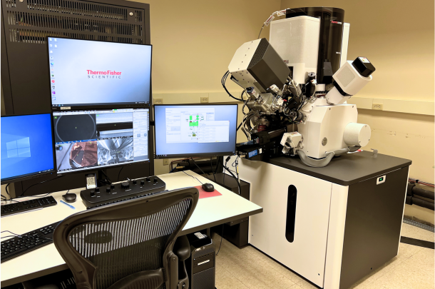
Electron beam resolution
- At optimum WD
- 0.7nm at 1 kV
- At coincident Point
- 0.6 nm at 15 kV
- 1.2 nm at 1 kV
Electron beam parameter space
- Electron beam current range: 0.8 pA to 100 nA at all accelerating voltages
- Accelerating voltage range: 350 V – 30 kV
- Landing energy: 20* eV – 30 keV
- Maximum horizontal field width: 2.3 mm at 4 mm WD
Ion Optics
High-performance PFIB column with unique Inductively Coupled Plasma (ICP) source supporting four ion species with fast switching capability
- Ion species (primary ion beam): Xe, Ar, O, N
- Switching time <10 minutes, only software operation
- Ion beam current range: 1.5 pA to 2.5 µA
- Accelerating voltage range: 500 V – 30 kV
- Maximum horizontal field width: 0.9 mm at beam coincidence point
Xe ion beam resolution at coincident point
- <20 nm at 30 kV using preferred statistical method
- <10 nm at 30 kV using selective edge method
Detectors
- Elstar in-lens SE/BSE detector (TLD-SE, TLD-BSE)
- Everhart-Thornley SE detector (ETD)
- IR camera for viewing sample/column
- High-performance In-Chamber Electron and Ion Detector (ICE), for secondary ions (SI) and electrons (SE)
- In-Chamber Thermo Scientific Nav-Cam™️ Sample Navigation Camera
- Retractable low-voltage, high-contrast directional solid-state backscatter electron detector (DBS)
- Integrated beam current measurement
Analytical Detectors
- EDAX Octane Elite Super EDS
- EDAX Velocity Ultra EBSD
Stage and Sample
High-precision, five-axis motorized stage with Piezo-driven XYR axis
- XY range: 150 mm
- Z range: 10 mm
- Rotation: 360° (endless)
- Tilt range: -38° to +60°
- XY repeatability: 1 μm
- Max sample height: Clearance 55 mm to eucentric point
- Max sample weight at 0° tilt: 500 g (including sample holder)
- Max sample size: 150 mm with full rotation
- Compucentric rotation and tilt
Chamber
- E- and I- beam coincidence point at analytical WD (4 mm SEM)
- Ports: 21
- Inside width: 379 mm
- Integrated plasma cleaner
